Topics
Characterisation of materials
Polymers (GRC)
| - |
In South Hadley, MA
Synthetic and Biologically-Derived Polymers
Characterisation of Materials used in Nuclear Environments
|
In London
Liquid Crystals (GRS)
| - |
In Biddeford, ME

CERMODEL - Modelling and Simulation Meet Innovation in Ceramics Technology
| - |
In Trento
Topics of interest
- Prediction/simulation of crystal structure and properties of advanced ceramics
- Characterization and modeling of surfaces, interfaces and grain boundaries at multiple scales in ceramics
- Modeling and simulation of grain growth and microstructure evolution in ceramics
- Virtual material design for new innovative materials
- Novel simulation methods for ceramic processing: shaping and sintering
- Modeling and simulation for ceramic composite manufacturing
- Modeling and simulation for CMCs, UHTCs, and UHTCMCs
- Mathematical models of electrical and magnetic properties in ceramics
- Mathematical model of optical and physical properties in ceramics
- Materials design for extreme environments
- Simulation/characterization of mechanical and tribological behavior
- Simulation/characterization of material behavior at high-temperatures
- Improvement performance through prediction and modelling in refractories and clay-based ceramics
- New ceramics for renewable energy applications
21st National Seminar on Crystal Growth and Applications
| - |
In Tiruchichirappalli

40th Annual Meeting of the British Zeolite Association
| - |
In Preston
A special session chaired by one of the BZA founders, Prof Alan Dyer, will reflect on the past 40 years of the association.
Keynote Speakers:
- Dr Julien Haines, Institut Charles Gerhardt Montpellier, Université de Montpellier, France
- Prof Raul Lobo, Chemical and Biomolecular Engineering, University of Delaware, USA
- Dr Alvaro Mayoral, Advanced Microscopy Laboratory, Universidad de Zaragoza, Spain
- Final plenary speaker TBC
The First UAE Synchrotron User Meeting
|
In Dubai
The purpose of the workshop is to bring together the best scientists from the United Arab Emirates (UAE) and synchrotron experts and see how the most strategic fields for the UAEÂ can be addressed through synchrotron science. UAE scientists will include both national and non-national speakers. International top synchrotron experts will give a talk at the event.
One of the main points will be to understand what the requirements of the UAE scientists are in terms of synchrotron research (what types of beamlines, techniques, etc.). Once these are defined, we will try to understand what would be the best option in terms of costs and benefits for the UAE.

ICYRAM2016. International Conference of Young Researchers on Advanced Materials
| - |
In Bangalore
Topics
-
Electronic and Photonic Materials
- Silicon Germanium
- Oxide Electronics
- III-V and II-VI
- Graphene and Analogues
- Organic Electronics
- Photonic Materials
- Nanomaterials Synthesis & Solutions Route
- Nanomaterials Devices & Applications
- Nitride Electronics
-
Advanced Functional Materials
- Magnetic & Spintronics
- Hybrids & Composites
- Ferroics
- Superconductors
- Glasses
- Electro Ceramics
- Microwave Materials
-
Energy and Green Materials
- Photovoltaics
- Hybrids including Biomass-Based Material
- Batteries, Fuel Cells & Supercapacitors
- Thermoelectrics
-
Advanced Structural Materials
- Composites
- Light Metals & Alloys
-
Materials Modelling and Simulation
- Computational Materials Science
- Simulation & Modelling
-
Materials Characterization
- Electron Microscopy
- Scanning Probe Microscopy
- Spectroscopy
-
Materials for Bio / Medical Applications
- Bio-sensors and probes
- Nanomedicine - Tissue Engineering
- Cell-Material Interaction
MS & T16. Materials Science & Technology
| - |
In Salt Lake City, UT
Organized in a joint partnership between four leading materials science-related societies â€" ACerS, AIST, ASM International, and TMS.
TECHNICAL PROGRAM
- Additive Manufacturing
- Biomaterials
- Ceramic and Glass Materials
- Electronic and Magnetic Materials
- Energy
- Fundamentals, Characterization, and Computational Modeling
- Iron and Steel (Ferrous Alloys)
- Materials-Environment Interactions
- Nanomaterials
- Processing and Manufacturing
- Special Topics

Electronic Materials and Applications 2017
| - |
In Orlando, FL
Symposia
- S1: Advanced electronic materials: processing, structures, properties, and applications
- S2: Advanced processing for electronic and electrochemical systems: crystals, films, and devices
- S3: Ceramic photonic materials and applications
- S4: Computational design of electronic materials
- S5: Energy sustainable optoelectronics and magnetoelectronics
- S6: Fundamentals to applications for the use of thermal energy for power generation and refrigeration
- S7: In situ experiments of microstructure evolution and properties
- S8: Interfaces and surfaces in energy-related ceramic materials
- S9: Interfaces in microstructural evolution: structure, properties, anisotropy, and motion
- S10: Interfacial phenomena in multifunctional heterostructures: from theory to transport processes
- S11: Ion conducting ceramics
- S12: 5G materials for the millimeter wave revolution
- S13: Mesoscale phenomena in ceramic materials, nano- and microstructures
- S14: Multifunctional nanocomposites
- S15: Superconducting materials and applications
- S16: Failure: the greatest teacher
2017 International Conference on Frontiers of Characterization and Metrology for Nanoelectronics (FCMN)
| - |
In Monterey, CA

NANOCON 2016 8th International Conference on Nanomaterials - Research & Application
| - |
In Brno
Plenary Session
Elementary Electronic Processes in Carbon-based Materials and Beyond: What do we Learn from Theory?
Â
With 2D Layers to New Compound Materials
- Session A - Nanomaterials for Electronic, Magnetic and Optic Applications. Carbon Nanostructures, Quantum Dots
- Session B - Industrial and Environmental Applications of Nanomaterials
- Session C - Bionanotechnology, Nanomaterials in Medicine
- Session D - Monitoring and Toxicity of Nanomaterials
- Session E - Advanced Methods of Preparation and Characterization of Nanomaterials

Epitaxie von III/V - Halbleitern (Epitaxy of III / V - semiconductors)
| - |
In Duisburg
Herstellung und Charakterisierung von massiven Halbleitern (Preparation and characterization of solid semiconductors
| - |
In Erlangen
21st American Conference on Crystal Growth and Epitaxy (ACCGE-21) and 18th US Workshop on Organometallic Vapor Phase Epitaxy (OMVPE-18)
| - |
In Santa Fe, NM
Workshop on high-pressure multigrain crystallography
| - |
In Argonne, IL
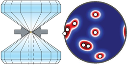
With the developments in micro-beam technology many traditional high-pressure powder samples may contain only tens or hundreds of multiple grains, displaying “spotty†poor powder patterns in diffraction images. As a result, polycrystalline structural refinement for ultrahigh-pressure samples becomes increasingly difficult and the results could be uncertain. On the other hand, successful examples of growth and preservation of micron-sized single crystal samples above 100 GPa are challenging and extremely rare. The recently developed “multigrain crystallography†treats multiple grains as a collection of single crystallites, obtaining diffraction data from a few to hundreds of single crystallites simultaneously. The multigrain approach provides great promise for structure refinement of miniature samples at ultrahigh pressures. This workshop will bring scientists from multiple disciplinary fields to (1) discuss the current status of multigrain crystallography, (2) review the currently used algorithms and various experimental procedures at synchrotron facilities, and (3) identify the challenges and opportunities of multigrain crystallography in high pressure research. Both the diffraction techniques using monochromatic and polychromatic beams will be discussed in this two-day forum.
The workshop contents:
- Â Plenary sessions with invited speakers, first day
- Â Discussions, second day
- Â Promises and limitations
- Â Indexation
- Â Integration filtering and scaling
- Â 2D/3D information
- Â Challenges and opportunities for high-pressure research
A registration fee of $150 will be assessed to all attendees except invited speakers. Â This fee includes the cost of meals, coffee breaks, and an abstract volume. Registration fee paid via PayPal (Visa and Mastercard accepted).
Organizing Committee
- Dmitry Popov (HPCAT), dpopov@carnegiescience.edu
- Guoyin Shen (HPCAT), gshen@carnegiescience.edu
- Stas Sinogeikin (HPCAT), ssinogeikin@carnegiescience.edu
- Przemek Dera (University of Hawaii at Manoa), pdera@hawaii.edu
Local Administrator
Freda Humble, (630) 252-0479, fhumble@ciw.edu  Workshop contact: multigrainworkshop2016@carnegiescience.eduÂ
DISCUS Workshop
| - |
In Erlangen
Within this workshop you will get an opportunity to learn all about structure simulation using DISCUS (https://github.com/tproffen/DiffuseCode ), a program complementary to the Rietveld approach. DISCUS can simulate powder pattern for disordered materials, crystalline and nanocrystalline.
In this workshop you will learn to interpret diffuse scattering and to simulate disordered crystal structures.Â
Defects are quite common in crystals and are responsible for a number of properties like ionic conductivity, electronic properties of indirect semiconductors etc.Â
In diffraction, defects manifest themselves by the presence of diffuse scattering. While its peak intensity usually is weak, the total scattering intensity will be an appreciable fraction of the Bragg intensities.Â
Thus, the description of these structures is largely incomplete without proper interpretation of the diffuse scattering.
The workshop covers the techniques to simulate and to refine disordered structures for a wide range of defects, and the corresponding calculation of the diffraction pattern for single crystals and powder, as well as the calculation of the pair distribution function PDF.
For more info please visit:
http://www.lks.physik.uni-erlangen.de/DISCUS/index.html
E-MRS Fall Meeting
| - |
In Warsaw
E-MRS Spring Meeting and Exhibit
| - |
In Strasbourg